Panasonic Announces 8K 36 Megapixel Global Shutter Organic Sensor… and Time To Stop Sony’s Sensor Hegemony

Organic Sensor
Rarely the development of a new sensor technology has been officially announced so often like the one of the organic sensor.
It started back in 2013 with Panasonic/Fujifilm. Official statements about its development continued to be published ever since by both, Fujifilm and Panasonic (full list at the very bottom of this article).
And now comes the next official press release. This time Panasonic says that “it has developed” an organic sensor with the following main characteristics:
- Organic Sensor
- 8K
- 36 Megapixel
- Global Shutter
- OPF CMOS image sensor design technology
- electronically-controlled variable ND filter function
- In-pixel capacitive coupled noise cancellation technique
- In-pixel gain switching technology
- Voltage controlled sensitivity modulation technology
You will find a more detailed description in the full press release below.
In the press release, Panasonic writes:
“we will utilize this OPF CMOS image sensor technology in various applications such as broadcasting cameras, surveillance cameras, industrial inspection cameras, automotive cameras, etc., and will contribute to realize high resolution, high speed and high precision imaging and sensing functions.”
They do not explicitly mention “digital photocameras“, but 43rumors specualtes that this could already be the sensor of the Panasonic GH6, which will shoot 8K video.
We know that the organic sensor is interesting also for the photography industry, since a Fujifilm managers said in 2016 here:
“We don’t have any specific plans of incorporating an organic sensor into our products at the moment, but yes we are observing the progress of this technology. As of today, there would be No benefits to using an organic sensor. Our X-Trans III sensor is superior to the currently available organic sensor.”
At this stage, I’m not sure if Panasonic and Fujifilm are still developing this sensor together. The original press-release of their organic sensor partnership has been taken down.
However, Fujifilm is still investing R&D into the organic sensor, as we could read from their press-release back in February 2017, where they announced the development of world’s fastest organic CMOS circuit for multi-bit flexible temperature sensor.
Sony Sensor Hegemony
Don’t get me wrong, Sony makes the best sensors, so Fujifilm should buy them from Sony (as they do now), but we definitely need more competition in a market dominated by Sony (especially since Sony bought Toshiba sensor business, who made Fuji’s 2/3 sensors).
TowerJazz, Samsung, and maybe soon the organic sensor by Panasonic and Fujifilm, are all welcome alternatives.
Currently, Sony can set the sensor price almost to their pleasure. With more competition, they will have to lower the price in order to keep their customers.
And of course, the best solution would be if Fujifilm (maybe together with Panasonic) can finally manufacture their own (organic) sensors, which on paper has impressive specs and would definitely be a game changer in the industry.
Of course, Sony is working on its own organic sensor, too, as a FR-reader reminded us in the comments. But I think it would be better for Fujifilm / Panasonic to have their own sensor.
With all that said, here is the Panasonic press release.
Panasonic Press Release
Panasonic Develops Industry’s-First*1 8K High-Resolution, High-Performance Global Shutter Technology using Organic-Photoconductive-Film CMOS Image Sensor
The new technology enables 8K high resolution and high picture quality imaging without motion distortion, even in extremely bright scenes.
Osaka Japan, – Panasonic Corporation today announced that it has developed a new technology which realizes 8K high-resolution (36M pixels), 60fps framerate, 450k high-saturation electrons and global shutter [1] imaging with sensitivity modulation function simultaneously, using a CMOS image sensor with an organic photoconductive film (OPF). In this OPF CMOS image sensor, the photoelectric-conversion part and the circuit part are independent. By utilizing this OPF CMOS image sensor’s unique structure, we have been able to newly develop and incorporate high-speed noise cancellation technology and high saturation technology in the circuit part. And, by using this OPF CMOS image sensor’s unique sensitivity control function to vary the voltage applied to the OPF, we realize global shutter function. The technology that simultaneously achieves these performances is the industry’s first*1.
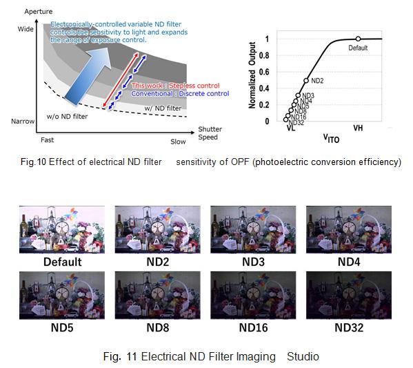
With the technology, it is possible to capture images at 8K resolution, even in high contrast scenes, such as a field under strong sunlight and shaded spectator seats under a stadium roof. Moreover, by utilizing the global shutter function that enables simultaneous image capture by all pixels, it is expected to be able to capture moving objects instantaneously without distortion, be utilized for multi viewpoint cameras (performing multi-view synchronized imaging using plural cameras) and used in fields requiring high-speed and high-resolution, such as machine vision and ITS monitoring. In addition, conventionally, even in scenes where it was necessary to utilize different ND filters [2] according to capturing conditions, the technology realizes a new electronically-controlled variable ND filter function which enables stepless adjustment of the OPF sensitivity [3] merely by controlling the voltage applied to the OPF.
The new technology has the following advantages.
8K resolution, 60fps framerate, 450k saturation electrons and global shutter function are realized simultaneously.
Switching between high sensitivity mode and high saturation mode is possible using gain switching function.
The ND filter function can be realized steplessly by controlling the voltage applied to the OPF.
This Development is based on the following technologies.
“OPF CMOS image sensor design technology”, in that, the photoelectric-conversion part and the circuit part can be designed independently.
“In-pixel capacitive coupled noise cancellation technique” which can suppress pixel reset noise at high speed even at high resolution
“In-pixel gain switching technology” that can achieve high saturation characteristics
“Voltage controlled sensitivity modulation technology” that can adjust the sensitivity by changing the voltage applied to the OPF.
Panasonic holds 135 Japanese patents and 83 overseas patents (including pending) related to this technology.
Panasonic will present some of these technologies at the international academic conference: ISSCC (International Solid-State Circuit Conference) 2018 which will be held in San Francisco on February 11 – 15, 2018.
Notes:
*1: As of February 14, 2018, according to Panasonic data.
More on the Technology
1. “OPF CMOS image sensor design technology”, in that, the photoelectric-conversion part and the circuit part can be designed independently.
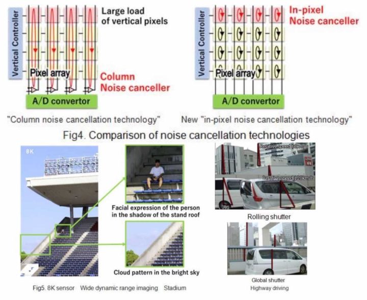
The OPF CMOS image sensor has a unique structure, in which, the OPF performs a photoelectric conversion and the circuit area performs charge storage and signal readout functions completely independently. Using this OPF CMOS image sensor structure, we developed high-speed noise cancellation technology and high saturation technology in the circuit area which has a large available space. As a result, it is possible to realize simultaneously 8K resolution, 60fps framerate readout, wide dynamic range [4] (by achieving a high saturation level) and global shutter function, which are normally traded off.


2. “In-pixel capacitive coupled noise cancellation technique” which can suppress pixel reset noise at high speed even at high resolution
Because the OPF CMOS image sensor has a structure in which the OPF and the charge storage part are connected by metal plugs, accumulated charges cannot be completely read out. Therefore, there is a problem that it is affected by reset noise at the time of resetting the pixel (signal charge storage node). And, in a high-resolution sensor, such as an 8K sensor, it is necessary to drive large loads exceeding 4000 pixels aligned in the vertical direction at the same time as the time of noise cancellation, and therefore, the long time it takes to suppress noise is a problem. So, we developed a new structure that cancels pixel reset noise at high speed, even when high resolution pixels have to be driven, by using Panasonic’s original semiconductor device technology and the newly developed “in-pixel capacitive coupled noise canceller”. In this structure, the reset noise is suppressed at high speed by using the negative feedback loop provided for each pixel.

3. “In-pixel gain switching technology” that can achieve high saturation characteristics
In the OPF CMOS image sensor, by incorporating a large capacitor in the circuit part with a large available area, it is possible to realize both high sensitivity mode and high saturation mode with the same pixel structure merely by switching modes from the camera system. In the high sensitivity mode, it is possible to capture data up to a light intensity of 4.5k electrons with high sensitivity. Furthermore, by switching to the high saturation mode, it is possible to capture data up to a light intensity of 450k electrons. In this way, since the high saturation mode can capture up to 10 times the high sensitivity mode, it is possible to clearly display the fine winding structure of the lamp filaments, in which bright part gradation cannot be expressed, because it becomes overexposure in high sensitivity mode, as shown in Fig. 3 (a). Even in a scene with high contrast, such as shown in Fig. 5, from the facial expression of the person in the shadow of the stadium roof to the blue sky and clouds during a mid-summer day, and such as shown in Fig. 6, from the dimly lit room to the sunny garden, it will be possible to capture brilliant images without overexposure or underexposure.

4. “Voltage controlled sensitivity modulation technology” that can adjust the sensitivity by changing the voltage applied to the OPF.
The OPF CMOS image sensor can change the sensitivity of the OPF simply by controlling the voltage applied to the OPF. By utilizing this function, we can realize the following functions which could not be realized with conventional silicon image sensors.
Sensitivity Modulation Example 1: Global shutter function which can capture all pixels simultaneously at 8K resolution
By controlling ON / OFF of the voltage applied to the OPF and controlling the sensitivity of the OPF, we realize the “global shutter function” capable of imaging all pixels at the same time, even driving a large number of pixels like the 8K sensor. By capturing with the global shutter function, as shown in Fig. 3 (b-43rumors), the letters on the rotating body are read sharply without distortion. In addition, as shown in Fig. 7, even at the time of high speed moving object capturing, such as when driving on a highway or at industrial inspection, capturing without distortion becomes possible.

In the conventional global shutter type silicon image sensor, it is necessary to add new elements such as transfer circuits and charge storage capacitors in order to accumulate charges simultaneously in all pixels. As a result, the area of the photodiode and that of the additional circuits must compete for space, there is a problem that the pixel size cannot be reduced and the amount of saturation electrons cannot be increased. On the other hand, in the OPF CMOS image sensor, since there is no need for additional elements, it is possible to realize small cell, high resolution sensors, and by incorporating large capacitors in the circuit part with a large available area, accurate imaging with no distortion from dark scenes to extremely bright scenes is possible. For example, as shown in Fig. 9, with the OPF CMOS image sensor, when buildings are photographed while panning [5-43r] at high speed, even in scenes with high contrast like a bright sky and dark windows, it is possible to acquire image data maintaining all gradations of the whole area without distortion.

Sensitivity Modulation Example 2: “Electrical ND Filter Technology” which can change sensitivity continuously and steplessly
Conventionally it has been necessary to provide a plurality of ND filters according to photographing conditions and change them many times. On the other hand, in the OPF CMOS image sensor, merely by controlling the voltage applied to the OPF (VITO in Fig. 8) and changing the sensitivity of the OPF to the desired value, it is possible to electrically implement the ND filter function. By using this function, it becomes possible to simplify the photographic equipment and continuously, steplessly control the sensitivity which could not be realized with a conventional silicon sensor. Therefore, the possibility of capturing according to the scene is expanded.
In the future, we will utilize this OPF CMOS image sensor technology in various applications such as broadcasting cameras, surveillance cameras, industrial inspection cameras, automotive cameras, etc., and will contribute to realize high resolution, high speed and high precision imaging and sensing functions.
Technical Terms:
[1] Global shutter:
Shutter operation which can captures the image at the same time with all pixels. Organic CMOS image sensors operate in rolling shutter mode in which exposure and shutter operation is executed row by row.
[2] ND filter
Abbreviated name of neutral density filter.
A filter that functions to evenly absorb light in the visible range and reduce only the light intensity without affecting color.
[3] Sensitivity modulation
The photoelectric conversion efficiency is changed according to the control. In the OPF CMOS image sensor, the photoelectric conversion efficiency can be changed by controlling the voltage applied to the OPF.
[4] Dynamic Range
Range of brightness that can be imaged.
(Ratio between the largest and the smallest values of brightness.)
[5] Panning
A technique for capturing wide scenes by moving the framing in the horizontal direction with a fixed camera, which is a common video capturing technique.
- June 2013: Fujifilm and Panasonic announced the organic sensor development
- June 2013: X-guru Rico Pfirstinger expected “actual digital cameras to feature this sensor design within 18-24 months from now”
- December 2014: Our sources told us here, that there is a crucial problem to be solved with the organic sensor: heat generation (and battery drain)
- December 2014: Top Fujifilm Managers confirmed, that the organic sensor is “still well ahead of us.”
- October 2015: 43rumors broke the rumor here, that it will still take a 2 or 3 years before the organic sensor will be ready for mass production.
- February 2016: Panasonic announced that, along with Fujifilm, they are developing an organic sensor with global shutter and impressive 123dB (!!!) dynamic range.
- February 2016: Fujifilm managment says: “We don’t have any specific plans of incorporating an organic sensor into our products at the moment, but yes we are observing the progress of this technology. As of today, there would be No benefits to using an organic sensor. Our X-Trans III sensor is superior to the currently available organic sensor.”
- March 2016: a source told us in March 2016 here, that the Global Shutter should find its way in the first cameras in 2018. But note that the source only said something about the global shutter, and not about the organic sensor.
- February 2017: Panasonic announces the world’s first organic CMOS image sensor with electrically controllable near-infrared light sensitivity. However, unlike in previous press-releases, this time Fujifilm isn’t mentioned.
- February 2017: Fujifilm Announces Development of World’s fastest Organic CMOS Circuit For Multi-bit flexible Temperature Sensor
- August 2017: Development of Wide Dynamic Range and Global Shutter Technology for Organic Photoconductive Film Image Sensor (Panasonic)
- February 2018: Panasonic Announces 8K 36 Megapixel Global Shutter Organic Sensor