Fujifilm Stacked sensor Patent (for Fujifilm X-H2S)

A patent has surfaced of a stacked sensor Fujifilm camera.
The patent itself says nothing about the Fujifilm X-H2, or megapixel or anything. It basically just explains the function of a stacked sensor in general, which we already know.
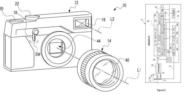
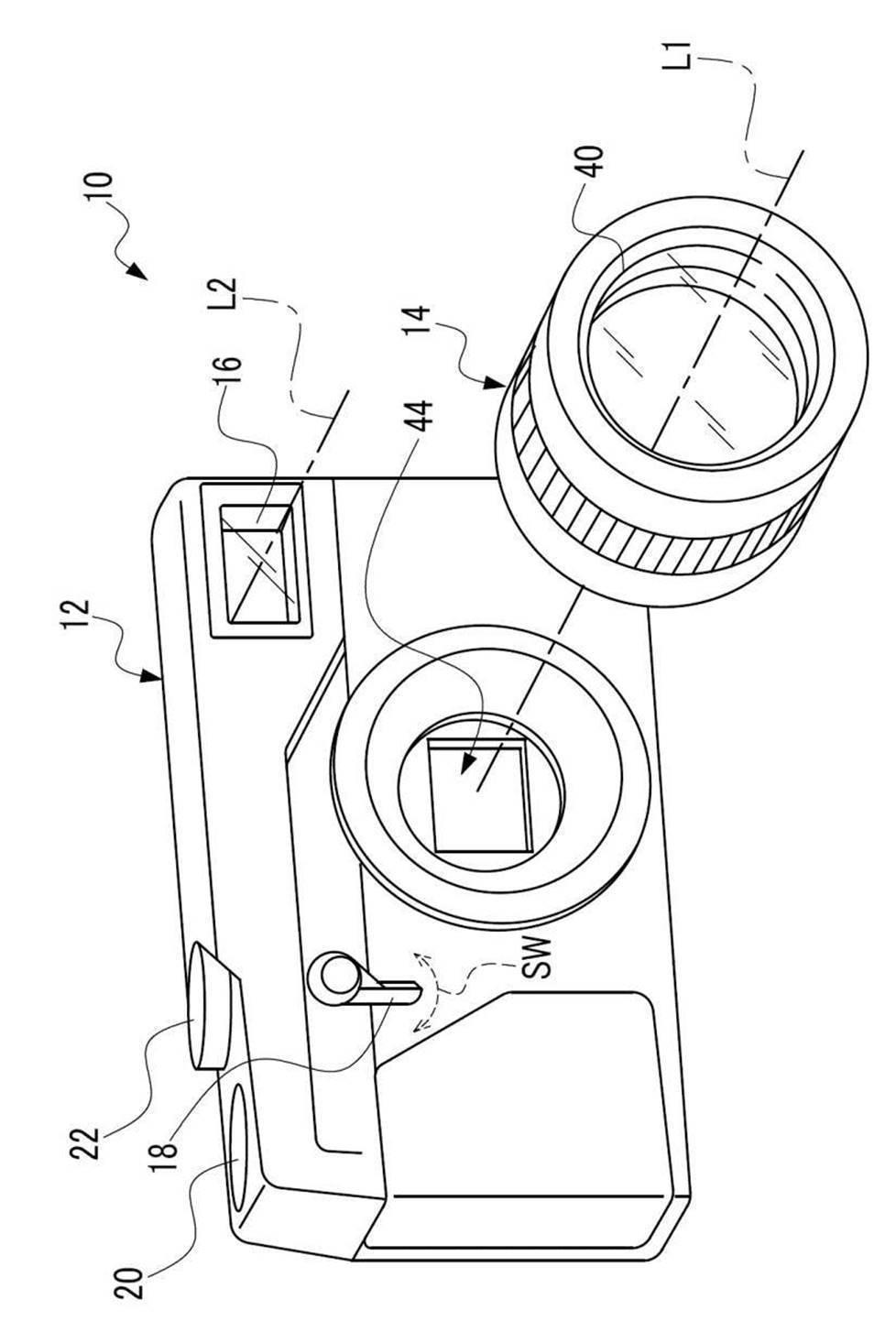
Also, they use a rangefinder camera to explain the patent… but that does not mean the next camera will be stacked sensor Fujifilm X-Pro4 ;).
We know that a stacked sensor is coming since 5th generation BSI stacked sensor camera. And we know it will be for the 26 megapixel Fujifilm X-H2S since earlier today (remains to see if also for the Fujifilm X-H2 high resolution).
The patent itself is an endless flow of technical functional details that do not say anything about what the camera is and its specs. But if you are an engineer and maybe love to dive deep into the technical side of things, you can find an except and the link down below.
Stay tuned… so much more is coming ;). Not complicated patents that do not say anything, but solid rumors that will give you a clear idea on what Fujifilm has planed to make Fuji X and GFX shooters happy ;).
Patent
(19) [Publication country] Japan Patent Office (JP)
(12) [Kind of official gazette] Published unexamined patent application (A)
(11) [Publication number] JP 2022 – 62138A (P2022-62138A)
(43) [Date of publication of application] Reiwa 4(2022) April 19 (2022.4.19)
(54) [Title of the invention] An imaging device, imaging apparatus, method of operating the imaging device, and program
(51) [International Patent Classification]
H04N 5/369 (2011.01)
H04N 5/225 (2006.01)
H04N 5/232 (2006.01)
[FI]
H04N 5/369
H04N 5/225 300
H04N 5/232 300
(21) [Application number] Japanese Patent Application No. 2022-13710 (P2022-13710)
(22) [Filing date] Reiwa 4(2022) January 31 (2022.1.31)
(62) [Display of division] Divisional application of P2021-501767
[Original Filing date] Reiwa 2(2020) January 28 (2020.1.28)
(31) [Application number of the priority] Japanese Patent Application No. 2019-28842 (P2019-28842)
(32) [Priority date] Heisei 31(2019) February 20 (2019.2.20)
(33) [Priority claim country/region or organization] Japan (JP)
(71) [Applicant]
[Identification Number]306037311
[Name]FUJIFILM CORP.
(72) [Inventor] [Name]KOBAYASHI, Sei
(72) [Inventor] [Name]Kawai Tomoyuki
(72) [Inventor] [Name]The history of cherry tree Takehito
(72) [Inventor] [Name]HASEGAWA, Ryo
(72) [Inventor] [Name]Sugawara One sentence
(57) [Overview] (Modified)
[Problem] To provide an imaging element capable of suppressing stagnation of output of image data, its operation method, and a program.
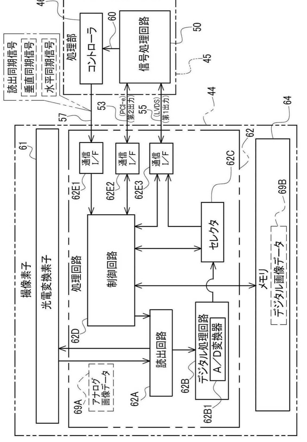
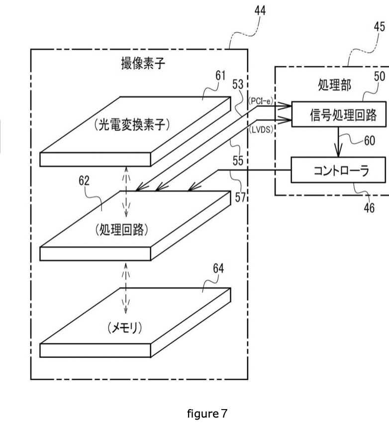
[Means for solving] In an imaging device, an imaging element outputs a 1 image data based on image data obtained by imaging an object to an external processor and a 1 communication interface 62 included in an imaging element. The image data is stored in the image pickup device and the 2 image data based on the image data stored in the memory is output to an external processor and the 2 communication interface 62 e2 built in the image pickup device is provided ; FIG. 1 is a block diagram of a 2 communication interface according to an embodiment of the present invention ;.
[Selected drawing] Fig.8
An imaging device includes a memory built in or connected to the processor, and a memory.
The processor and the memory are incorporated in the imaging element.
The processor has a 1 communication interface and a 2 communication interface.
The 1 communication interface outputs image data obtained by capturing an image of an object to a 1 external processor disposed outside the imaging element as the 1 image data.
The memory stores the image data.
The 2 communication interface outputs the image data stored in the memory as 2 image data to a 2 external processor.
The output system of the 1 communication interface is different from the output system of the 2 communication interface.
The 1 communication interface outputs the image data transferred without passing through the memory as the 1 image data.
An image pickup device.
[Claim 2] The imaging device according to claim 1, wherein output of the 1 image data by the 1 communication interface and output of the 2 image data by the 2 communication interface are performed independently of each other.
[Claim 3] The imaging device according to claim 1, wherein the 1 communication interface outputs the 2 image data in a period different from an output period of the 2 image data by the 1 communication interface.
[Claim 4] The imaging device according to claim 3, wherein the 2 communication interface outputs the 2 image data in response to a request from the external processing unit.
[Claim 5] The imaging device according to claim 3 or 4, wherein the output period is a vertical blanking period after the 1 image data for 1 frames is output from the 1 communication interface.
[Claim 6] The imaging device according to claim 3 or 4, wherein the output period is a vertical blanking period before the 1 image data for 1 frames is output from the 1 communication interface.
[Claim 7] The imaging device according to claim 3 or 4, wherein the output period is a horizontal blanking period after the 1 image data for 1 lines is output from the 1 communication interface.
[Claim 8] The imaging device according to claim 3 or 4, wherein the output period is a horizontal blanking period before the 1 image data for 1 lines is output from the 1 communication interface.
[Claim 9] The device includes a 1 A / D converter for performing A / D conversion of analog image data.
The imaging device according to claim 3 or 4, wherein the output period is an A / D conversion period by the 1 A / D converter before the 1 image data for 1 lines is output from the 1 communication interface.
[Claim 10] The device includes a 2 A / D converter for performing A / D conversion of analog image data.
The processor includes a memory controller which causes the memory to store digital image data obtained by digitizing the analog image data by the 2 A / D converter.
The output of the 1 communication interface is obtained from the 2 A / D converter.
The output system outputs the digital image data as the 1 image data without storing the digital image data in the memory.
An imaging device according to any one of claims 1 to 9, wherein an output method of the 2 communication interface is an output method of outputting the digital image data read from the memory by the memory controller as the 2 image data.
[Claim 11]
An imaging device according to any one of claims 1 to 10, wherein the memory is a memory having a different write timing and a different read timing.
[Claim 12]
The imaging device of claim 11, wherein the memory is a DRAM.
[Claim 13]
An imaging device according to any one of claims 1 to 12, wherein at least the photoelectric conversion element and the memory are formed into 1 chips.
[Claim 14]
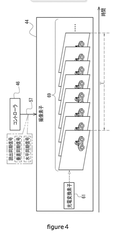
The imaging device according to claim 13, wherein the imaging element is a stacked imaging element in which the memory is stacked on the photoelectric conversion element.
[Claim 15]
An imaging device according to any one of claims 1 to 14.
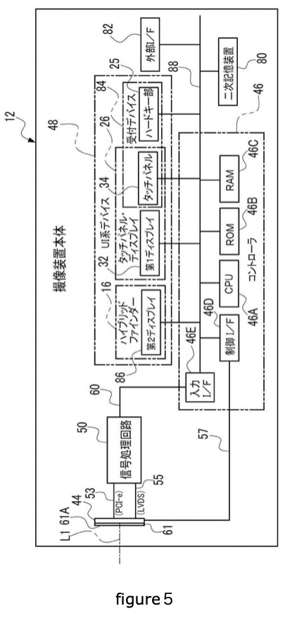
A display processor for controlling the display of at least one of a 1 image based on the 1 image data output by the 1 communication interface and a 2 image based on the 2 image data output by the 2 communication interface ;
An imaging apparatus comprising :.
[Claim 16]
An imaging device according to any one of claims 1 to 14.
A storage processor for controlling a storage device to store at least one of the 1 image data output from the 1 communication interface and the 2 image data output from the 2 communication interface ;
An imaging apparatus comprising :.
[Claim 17]
A method of operating an imaging device, comprising : a processor ; a memory built into or connected to said processor ; and a 1 communication interface and a 2 communication interface.
The 1 communication interface outputs, as 1 image data, image data obtained by imaging an object to a 1 external processor disposed outside the imaging element.
The memory stores the image data.
The 2 communication interface outputs the image data stored in the memory as 2 image data to a 2 external processor.
The output system of the 1 communication interface is different from the output system of the 2 communication interface.
The 1 communication interface outputs the image data transferred without passing through the memory as the 1 image data.
An operating method of an image sensor.
[Claim 18]
A program for causing a computer to function as the 1 communication interface and the 2 communication interface, wherein a processor and a memory built in or connected to the processor are incorporated, and the processor is included in an imaging element having a 1 communication interface and a 2 communication interface, is provided.
The 1 communication interface outputs, as 1 image data, image data obtained by imaging an object to a 1 external processor disposed outside the imaging element.
The memory stores the image data.
The 2 communication interface outputs the image data stored in the memory as 2 image data to a 2 external processor.
The output system of the 1 communication interface is different from the output system of the 2 communication interface.
The 1 communication interface outputs the image data transferred without passing through the memory as the 1 image data.
Program.
via j-platpat